At a former employer, they threw away a HP 4195A network analyser. The reason was because it had some problems with its internal source. I kept the unit for a few years and always was afraid of opening it and repairing it because I thought the potential to further damage it was too high. But now I tried to repair it and it worked 🙂
The problem with the source was that the output level dropped very abruptly above approx. 150 MHz and therefore the tracking generator and the network analyser functions were almost unusable. Here is a photograph of the unit in spectrum analyser mode with the source output connected to the receiver input:
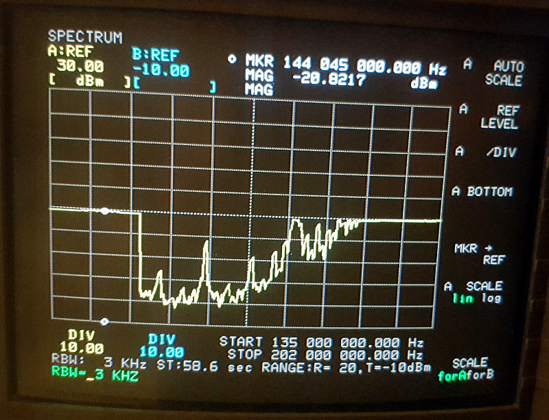
To check whether it was a problem with the receiver, I exchanged receiver inputs and connected the tracking generator to each of the 4 receiver inputs. The behaviour was the same on each receiver.
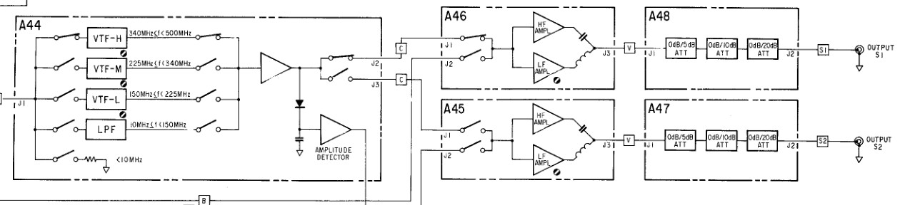
Further, I checked whether it was a problem with the source output. So I did the same check with the source output #2, but the result was still the same. A look in the block diagram shows that both source outputs are connected to a voltage tuned bandpass filter (A44) with kind of a multiplexer in between. Since the behaviour on both source outputs was the same, the A46 and A45 units cannot be faulty (otherwise they would have had the exact same problem, which I thought is unlikely).
So, I checked the tuning voltage for this voltage tuned bandpass filters. Here is the schematic of A44:
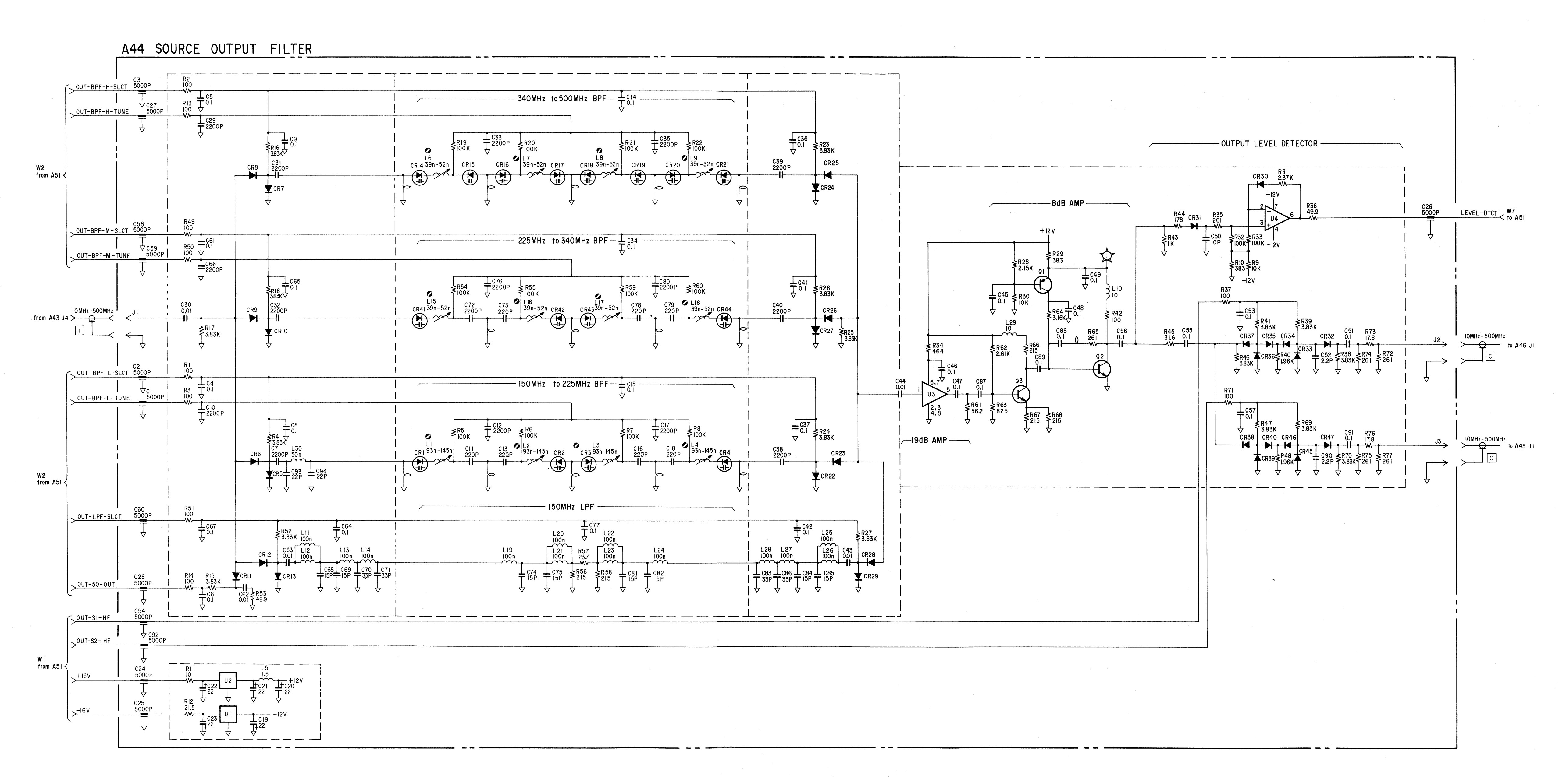
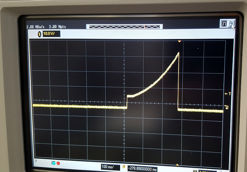
Apparently, the SLCT signals select which of the four filters is in the signal path, and according to their name, the TUNE signals tune the bandpass filters. So I measured both the TUNE as well as the SLCT signal with my scope, triggering on SLCT, and I saw this:

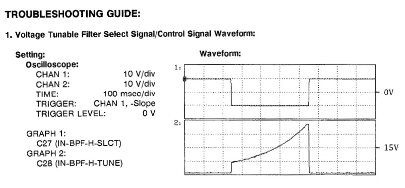
Oh shit, the upper trace doesn’t look so nice. The voltage is too low and the trace is kind of noisy. To verify whether there is actually a problem with the TUNE signal, I checked the TUNE signal for the A23 assembly, which is the receiver input filter and has the exact same filters on it. In the service manual, there is a scope pictutre how the signals should look like:
There is definitely a problem with the TUNE signal! The TUNE signal on A23 looked like this:
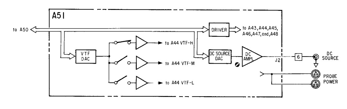
So, at least there is no problem with A23 and A50, which generates this tuning signal. But apparently, the problem must lie within A51 which is the source circuit control assembly. This board generates the tuning voltage for A44. This is the block diagram for A51:
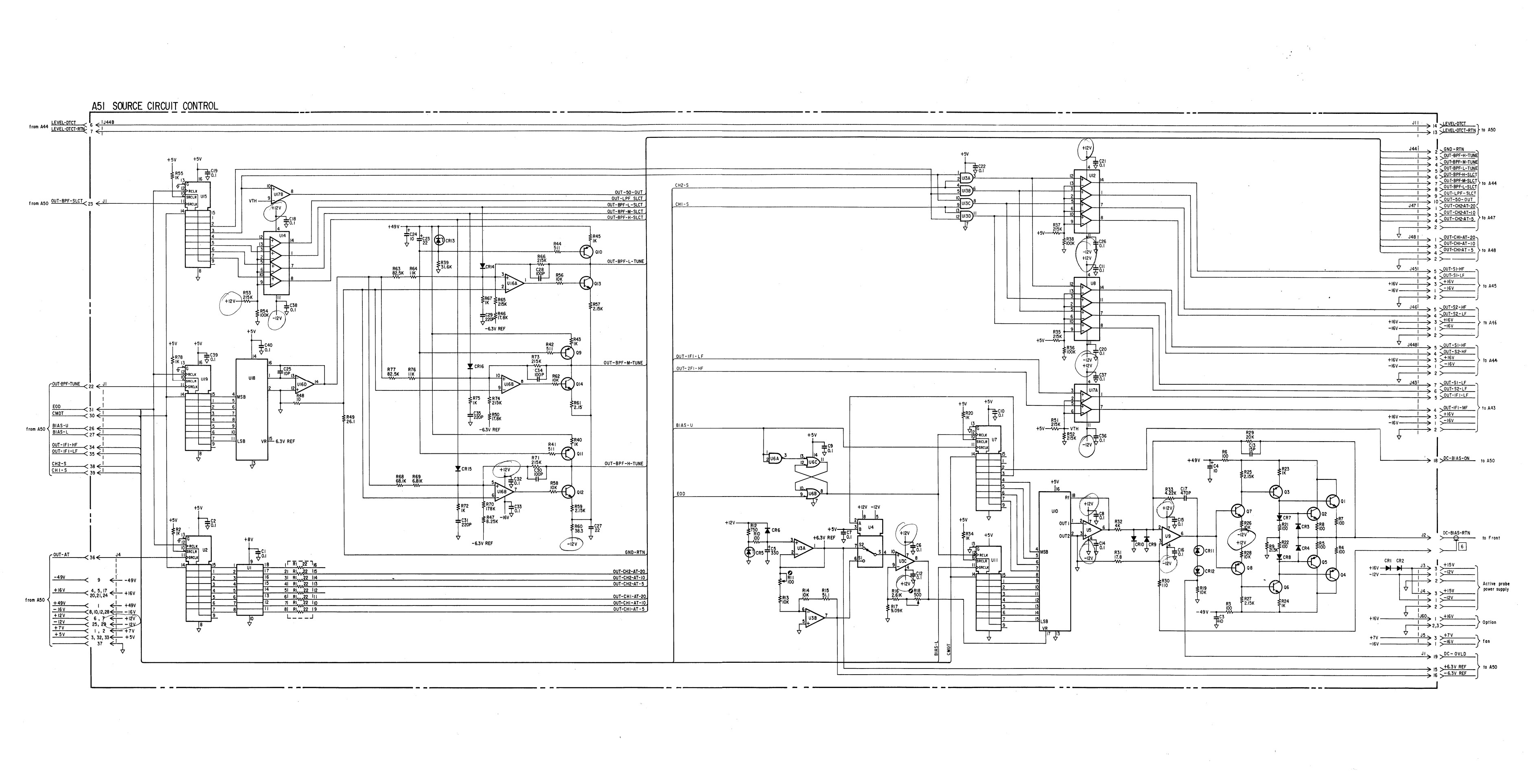
There could be a problem with the DAC or with the amplifiers. Because the TUNE signal looked exactly the same for bandpass filters, chances are high that the DAC has a problem. Here is the schematic of the questionable assembly:
I measured the output voltage of the OpAmp U16, which is a TL074 – same result! I guessed that U16 could be faulty. Because I had some TL074 at hand, I removed it and soldered a new one into the board. But this didn’t help. I was afraid that the DAC could be the problem.
The 4195A has a test mode which can be entered with the command ‘STSET’. Self Test #13 allows one to write binary data to the DAC. I wrote several values to it and tested whether the bit patterns correctly arrive at the DAC. This showed that there was no communication problem between the control unit and the measurement unit; whatever value I sent to the DAC, the correct bit pattern appeared at its 8 input pins.
At pin 14 of the DAC, one can measure the output voltage, and I saw that the output voltage didn’t correspond to the bit pattern! Here is what I measured at the DAC’s output:
| DAC Value | Output Voltage |
| 0 | 0 V (as expected) |
| 255 | -6.3 V (as expected; VREF is 6.3 V) |
| 1 | -300 mV (expected: 24 mV) |
| 128 | -3.15 V (as expected) |
| 129 | -3.45 V |
AHA! looks like the DAC is faulty. It is a AD7523 from Analog Devices; fortunately, there is the MX7523 from Maxim, which is still produced and is a pin compatible replacement for the AD7523. I ordered one of these MX7523, removed the old DAC and inserted the new one. Here are a few pics.
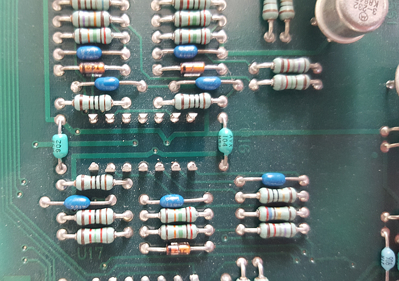
This is the assembly where the faulty DAC is located:

This was when I first thought that the OpAmp was faulty, and I removed it and soldered in a new one 🙂
After replacing the DAC, I turned on my 4195A, entered the spectrum analyser mode and checked what trace the tracking generator produces.
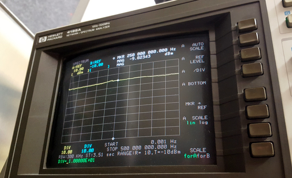
YAY! Seems like the problem is solved! The problem was definitely the broken DAC. I guess that due to aging some moisture could enter into the DACs package and therefore some of the internal resistors drifted – actually, the DAC was working, but output voltages were wrong, which is an indication that only the resistor values were wrong.
Now the 4195A can be used with the tracking generator, cool! unfortunately, it should be necessary to calibrate it again, because changing the DAC could alter the characteristic curve of the voltage tuned bandpass filters. In another post I will show how I reverse-engineered the calibration software!
